


State-of-the-Art Facility Marks a New Era in Innovation
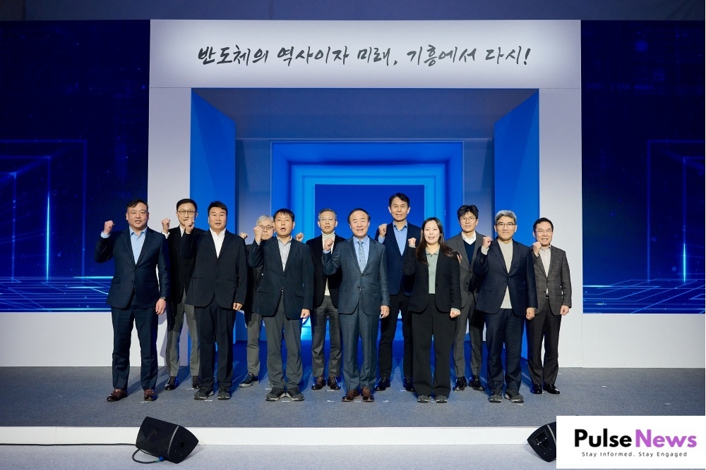
Samsung Electronics has officially marked a major achievement with the tool-in ceremony for its cutting-edge semiconductor research and development complex (NRD-K) at the Giheung campus. The event was attended by approximately 100 guests. Which is including suppliers and customers, who gathered to celebrate this significant moment in the company’s growth.
Paving the Way for Future Semiconductor Advancements
The NRD-K facility, which began construction in 2022, is poised to become a key hub for Samsung’s memory, system LSI, and foundry semiconductor research and development. Designed with advanced infrastructure, the complex will enable seamless research and product-level testing under one roof.
Samsung is investing an impressive KRW 20 trillion into the project by 2030, with the facility covering an expansive 109,000 square meters within the Giheung campus. A dedicated R&D production line is also expected to begin operation by mid-2025.
“NRD-K will accelerate our R&D efforts and help us create a continuous loop of innovation, driving next-generation technology research and large-scale production,” stated Young Hyun Jun, Vice Chairman and Head of the Device Solutions Division at Samsung Electronics. “”This new facility will allow us to build on the strong foundation established in Giheung. Which is the birthplace of Samsung’s semiconductor journey 50 years ago, while setting the stage for future innovations and growth.””
In addition, Park Gwang-Sun, Head of Applied Materials Korea, emphasized the importance of collaboration. Saying, “In today’s environment, win-win partnerships are crucial. We’re committed to accelerating innovation alongside Samsung Electronics and helping drive the next wave of growth in the semiconductor industry.”
The Giheung campus, situated south of Seoul, has long been a hub for revolutionary semiconductor developments. It includes the introduction of the first 64-megabit DRAM in 1992. It markes a pivotal moment in the industry’s history.
The new R&D complex will continue this legacy by introducing cutting-edge developments in process technology and manufacturing tools, solidifying the campus’s position as a leader in innovation.
NRD-K
NRD-K will feature state-of-the-art equipment such as High NA extreme ultraviolet (EUV) lithography and advanced material deposition tools. Its aim at accelerating the development of next-generation memory technologies like 3D DRAM and V-NAND with over 1,000 layers.
Additionally, the facility will incorporate advanced wafer bonding technology. It enables innovative wafer-to-wafer bonding capabilities.
Samsung has allocated substantial resources to research and development, with a record investment of KRW 8.87 trillion in the third quarter. This funding further bolsters its efforts to take the lead in cutting-edge technologies. These are the advanced packaging for high-bandwidth memory (HBM) production.


